
Gm 107 какая видеокарта
Сведения о типе (для десктопов или ноутбуков) и архитектуре GM107 и GeForce MX150 GP107, а также о времени начала продаж и стоимости на тот момент.
| Место в рейтинге производительности | не участвует | не участвует |
| Архитектура | Maxwell (2014−2018) | Pascal (2016−2021) |
| Графический процессор | GM107 | GP107 |
| Тип | Десктопная | Для ноутбуков |
| Дата выхода | нет данных | 23 февраля 2019 (3 года назад) |
| Цена сейчас | 11.37$ | нет данных |
Другие видеокарты
Здесь мы рекомендуем несколько видеокарт, более или менее близких по производительности к рассмотренной.
Сведения о типе (для десктопов или ноутбуков) и архитектуре GM107 и GK104, а также о времени начала продаж и стоимости на тот момент.
| Место в рейтинге производительности | не участвует | не участвует |
| Архитектура | Maxwell (2014−2018) | Kepler (2012−2018) |
| Графический процессор | GM107 | GK104 |
| Тип | Десктопная | Десктопная |
| Дата выхода | нет данных | нет данных |
| Цена сейчас | 11.37$ | 146$ |
Проголосуйте
Вы согласны с нашим мнением или думаете иначе? Проголосуйте за любимую видеокарту, нажав кнопку "Нравится".
Характеристики
Общие параметры GM107: количество шейдеров, частота видеоядра, техпроцесс, скорость текстурирования и вычислений. Они косвенным образом говорят о производительности GM107, но для точной оценки необходимо рассматривать результаты бенчмарков и игровых тестов.
| Количество потоковых процессоров | 640 | из 18432 (AD102) |
| Количество транзисторов | 1,870 млн | из 14400 (GeForce GTX 1080 SLI (мобильная)) |
| Технологический процесс | 28 нм | из 4 (H100 PCIe) |
Поддержка API
Перечислены поддерживаемые GM107 и GeForce MX150 GP107 API, включая их версии.
| DirectX | 12 (11_0) | нет данных |
| Шейдерная модель | 5.1 | 6.4 |
| OpenGL | 4.6 | нет данных |
| OpenCL | 3.0 | нет данных |
| Vulkan | 1.3 | 1.2.131 |
| CUDA | 5.0 | 6.1 |
Технологии
Здесь перечислены поддерживаемые GM107 и GeForce MX150 GP107 технологические решения и API. Такая информация понадобится, если от видеокарты требуется поддержка конкретных технологий.
| PureVideo HD | VP6 | нет данных |
Технические характеристики
Это важная информация, которая определяет все мощностные характеристики видеокарты NVIDIA GeForce GTX 750. Чем меньше технологический процесс изготовления чипа, тем лучше (в современных реалиях). Тактовая частота ядра отвечает за его быстродействие (прямая корреляция), в то время как обработка сигналов осуществляется транзисторами (чем больше транзисторов, тем быстрее выполняются вычисления, например в майнинге криптовалюты).
| Конвейеры: | 512 | |||
| Тактовая частота ядра: | 1020 MHz | |||
| Разгон: | 1085 MHz | |||
| Количество транзисторов: | 1,870 million | |||
| Технологический процесс: | 28 nm | |||
| Потребляемая мощность (TDP): | 55 Watt | |||
| Количество текселей, обрабатываемых за 1 секунду: | 34.72 | |||
| Операций с плавающей запятой: | 1,111 gflops | |||
| Максимальная температура: | 95 °C | |||
| Ядра CUDA: | 512 | |||
| Конвееров / CUDA ядер: | 512 | |||
| Скорость разгона: | 1085 MHz | |||
| Количество транзисторов: | 1,870 million | |||
| Расчетная тепловая мощность: | 55 Watt | |||
Преимущества и минусы
Technical City не может определиться с выбором между
и
У нас нет данных о результатах тестов, чтобы выбрать победителя.
Если у вас остались вопросы по выбору между GM107 и GK104 - задавайте их в комментариях, и мы ответим.
Проголосуйте
Вы согласны с нашим мнением или думаете иначе? Проголосуйте за любимую видеокарту, нажав кнопку "Нравится".
Память (частота и разгон)
Внутренняя память используется для хранения данных при проведении вычислений. Современные игры и профессиональные графические приложения предъявляют высокие требования к объему и скорости памяти. Чем выше этот параметр, тем мощнее и быстрее видеокарта. Тип памяти, объем и пропускная способность для NVIDIA GeForce GTX 750 + возможность разгона в турбо-режиме.
| Тип памяти: | GDDR5 | |||
| Maximum RAM amount: | 1 GB | |||
| Разрядность шины памяти: | 128 Bit | |||
| Частота памяти: | 5.0 GB/s | |||
| Пропускная способность памяти: | 80 GB/s | |||
Совместимость и размеры
Параметры, отвечающие за совместимость GM107 и GeForce MX150 GP107 с остальными компонентами компьютера. Пригодятся например при выборе конфигурации будущего компьютера или для апгрейда существующего. Для десктопных видеокарт это интерфейс и шина подключения (совместимость с материнской платой), физические размеры видеокарты (совместимость с материнской платой и корпусом), дополнительные разъемы питания (совместимость с блоком питания). Для ноутбучных видеокарт это предполагаемый размер ноутбука, шина и разъем подключения, если видеокарта подключается через разъем, а не распаивается на материнской плате.
| Интерфейс | нет данных | PCIe 3.0 x16 |
Общая игровая производительность
Все тесты основаны на показателях FPS. Давайте посмотрим, какое место заняла NVIDIA GeForce GTX 750 в тесте игровой производительности (расчет произведен в соответствии с рекомендациями разработчика игры по системным требованиям; он может отличаться от реальных ситуаций).
Это десктопная видеокарта на архитектуре Maxwell и техпроцессе 28 нм, в первую очередь рассчитанная на геймеров.
У нас нет данных о результатах тестирования GM107.
Related News
- Mar 1st 2022 NVIDIA DLSS Source Code Leaked (83)
- Jan 21st 2022 Intel Arc Alchemist Xe-HPG Graphics Card with 512 EUs Outperforms NVIDIA GeForce RTX 3070 Ti (95)
- Mar 26th 2022 NVIDIA GeForce RTX 4090/4080 to Feature up to 24 GB of GDDR6X Memory and 600 Watt Board Power (107)
- Jun 6th 2020 NVIDIA GeForce RTX 3080 Pictured? (225)
- Aug 22nd 2020 NVIDIA GeForce RTX 3090 Founders Edition Potentially Pictured: 3-slot Behemoth! (183)
- Dec 29th 2020 A Christmas Miracle: 500,000 NVIDIA RTX 3080 Cards Found in Lost Shipping Container (103)
- Jan 17th 2022 NVIDIA's Custom RTX 3090 Ti Graphics Cards Reach $4,000 Pricing in Europe (111)
- Apr 27th 2022 NVIDIA Allegedly Testing a 900 Watt TGP Ada Lovelace AD102 GPU (102)
- Dec 2nd 2021 NVIDIA GeForce RTX 2060 12GB Has CUDA Core Count Rivaling RTX 2060 SUPER (99)
- May 6th 2022 NVIDIA GeForce RTX 3090 Ti Gets Custom 890 Watt XOC BIOS (62)
Преимущества и минусы
Technical City не может определиться с выбором между
и
У нас нет данных о результатах тестов, чтобы выбрать победителя.
При этом необходимо отдавать себе отчет в том, что GM107 предназначена для настольных компьютеров, а GeForce MX150 GP107 - для ноутбуков.
Если у вас остались вопросы по выбору между GM107 и GeForce MX150 GP107 - задавайте их в комментариях, и мы ответим.
Технологии
Здесь перечислены поддерживаемые GM107 технологические решения и API. Такая информация понадобится, если от видеокарты требуется поддержка конкретных технологий.
| PureVideo HD | VP6 |
Технологии
Здесь перечислены поддерживаемые GM107 и GK104 технологические решения и API. Такая информация понадобится, если от видеокарты требуется поддержка конкретных технологий.
| PureVideo HD | VP6 | VP5 |
Поддержка API
Все поддерживаемые видеокартой NVIDIA GeForce GTX 750 API, перечислены ниже. Это малозначимый фактор, который не сильно влияет на общую производительность.
| DirectX: | 12 (11_0) | |||
| OpenGL: | 4.4 | |||
| Vulkan: | 1.1.126 | |||
| Shader Model: | 5.1 | |||
| OpenCL: | 1.2 | |||
Поддержка API
Перечислены поддерживаемые GM107 API, включая их версии.
| DirectX | 12 (11_0) |
| Шейдерная модель | 5.1 |
| OpenGL | 4.6 |
| OpenCL | 3.0 |
| Vulkan | 1.3 |
| CUDA | 5.0 |
Характеристики
Общие параметры GM107 и GeForce MX150 GP107: количество шейдеров, частота видеоядра, техпроцесс, скорость текстурирования и вычислений. Они косвенным образом говорят о производительности GM107 и GeForce MX150 GP107, но для точной оценки необходимо рассматривать результаты бенчмарков и игровых тестов.
| Количество потоковых процессоров | 640 | нет данных |
| Количество транзисторов | 1,870 млн | 3,300 млн |
| Технологический процесс | 28 нм | 14 нм |
| Скорость текстурирования | нет данных | 36.77 |
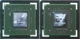
29 Comments on NVIDIA GM107 "Maxwell" Silicon Pictured
960 cores, over 1GHz gpu speed, 28nm for only 75W? If this is true then Nvidia did a little miracle here with Maxwell. The funny thing is that, if 75Ws are true, there is no reason for someone to buy a hi end card today. Either an AMD one or an Nvidia one. Even 790 or the new Titan will be old news before we even see a review of them. 6-9 months life at best for any card over $500 before it is obsolete. Because think Maxwell at 20nm.
john_960 cores, over 1GHz gpu speed, 28nm for only 75W? If this is true then Nvidia did a little miracle here with Maxwell.
Big_Vulture75W is good for laptops too. What was the power consumption for a similar performance Kepler card?
Between 114Ws (GTX 650ti - 768cores, 128bit, 928MHz) and 140Ws (GTX 660 - 960cores, 192bit, 980Mhz), I think closer to that 140W.
Looking at 700 series, GTX 760 is at 170W with "only" 192 more cores, 256bit data bus and 980MHz gpu speed.
It's definitely more power efficient. The specs they give for the GK106 are from the 660. From the leaked benchmarks it doesn't compete with it rather the 650 Ti

Big_Vulture75W is good for laptops too. What was the power consumption for a similar performance Kepler card?
VideoCardzThe footprint on power consumption will be dramatically lower than any Kepler GPU. In fact, most GeForce GTX 750 series cards will not require any power connectors, but of course there some with 6-pin installed.
Big_Vulture75W is good for laptops too. What was the power consumption for a similar performance Kepler card?
75W at this performance makes its really worthy and easy to put 2 of those on the same PCB, unless its not cost effective because it can be overpriced. we are talking about nvidia here.
Kaynar75W at this performance makes its really worthy and easy to put 2 of those on the same PCB, unless its not cost effective because it can be overpriced. we are talking about nvidia here.
The problem with the two cards idea is that Nvidia cut out the SLi support in the cheaper cards. Don't expect SLi support with these cards.
Didn't read correctly the part about "same PCB". I don't expect something like that anyway.
john_The problem with the two cards idea is that Nvidia cut out the SLi support in the cheaper cards. Don't expect SLi support with these cards.
Didn't read correctly the part about "same PCB". I don't expect something like that anyway.
Asus put two mid range GTX760 cores on the same PCB, so I was thinking they might do it again with these but at a very convenient price, and not $600+.
KaynarAsus put two mid range GTX760 cores on the same PCB, so I was thinking they might do it again with these but at a very convenient price, and not $600+.
Yes I realized what you where saying but, later, after posting. The problem with 750 is that it wouldn't support(I guess) SLi, so, is it possible to put two gpus that they possibly don't support SLi on the same PCB?
The fact that a card like this might cost about $250, maybe it wouldn't make it financially viable. Also it doesn't offer much as a publicity stunt. ASUS's card was fast enough to be advertised as "faster than Titan" this might be faster than 760 and with less power consumption, but not something that someone would be interested in buying. A single gpu is always preferable.
I can see clearly now that these GPUs are made for incoming slew of steam machines running on cheap TFX 150W PSUs
Being 75 watts is all PCI-e provides. would be a 6pin pci-e for it cause boost clock will put it over 75.
That new die size is much better suited to have ROI than the GK106 ever was for them! The 750 will be the 75W part, while the 750Ti could be as high as 110W.
So slighty smaller than the Bonaire XTX, with it's 115W TDP, and by the Fire Strike above much like a reference R7 260X.
Look at that valley score, this will compete with 7790 and maybe 260x at best.
Valley is the worst one by a long shot. The above scores vary 70-96% of the GTX 660. I'm guessing with real games with usable settings, it does better than what the Valley benchmark suggests. Push it, and 2/3 ROPs and 2/3 vram width shine through with a 70% result.
CasecutterThat new die size is much better suited to have ROI than the GK106 ever was for them! The 750 will be the 75W part, while the 750Ti could be as high as 110W.
FFS, how about dialling down the FUD for a change.
From the Videocardz link bta linked to, it clearly shows that the fully enabled (960 shader) die is ~75W. You also posted on the previous articlewhere the original SweClockers linkbta provided clearly stated:
Both graphics cards will also be without connections to external power supply , which ensures a maximum TDP of 75 watts.
All this, when every source seems to note that the cards leaked are overclocked SKUs, and still don't utilise anything other than the PCI-E slot for power.
:banghead:
HumanSmokeAll this, when every source seems to note that the cards leaked are overclocked SKUs, and still don't utilise anything other than the PCI-E slot for power.
Don't get that Chef's hat in such a wad.
I'm just reading the information as provided from both the TPU articles, and there’s always someone here to provide a alternate opinion. I'm not the only one on this thread that's skeptical of a Ti OC not needing the 6-Pin.
First, that “other” TPU article never mentions the TDP for either. I don't read Swedish and won't normally have time to translate every article, it's a shame that information was omitted within btarunrs’ re-write, take that up with him. If you look I wrote that several hour before the post here.
While yes I just miss-read it denoting the "Ti" designation; "The TDP of the GTX 750 Ti is approximated to be around 75 Watt". With all the designators Ti /non-Ti and former/latter bantered-about I just took away the wrong information, a simple mistake. While are you saying even the OC'd (and are you indicating Ti's) don't utilize anything other than the PCI-E slot power?
I'll hold to a wait and see as we know much of this communication get convoluted and mixed-up just as I have.
Might I suggest you actually read the source material - the original article links are provided for a reason. assuming you're actually interested of course
CasecutterI don't read Swedish and won't normally have time to translate every article it's a shame that information was omitted within btarunrs’ re-write, take that up with him.
Why? My schedule allowed for 75 seconds to translate the SweClockers article link that bta provided. I honestly didn't realise that Google translate, or copy/pasting a block of text into any other online translator was deemed such a time consuming business. Your life must be phenomenally busy, although I wonder how you couldn't budget a couple of minutes to translate and read a paragraph of source material, but could find the time to reply to my post
Which makes the post here all the more suspect, considering the article (and the SweClockers link provided) you earlier posted on had all the relevant information to hand.
CasecutterWhile yes I just miss-read it denoting the "Ti" designation; "The TDP of the GTX 750 Ti is approximated to be around 75 Watt".
The likely reason it is approximated is if the card does not a PCI-E power input, the cards draw is limited to a nominal 75W through the PCI-E x16 slot.
CasecutterWhile are you saying even the OC'd (and are you indicating Ti's) don't utilize anything other than the PCI-E slot power?
What I'm seeing is a low-end priced card with a 75W power budget with clocks of 1085MHz core/1163MHz boost. Now, there may well be SKUs with an auxiliary 6-pin power input. so what kind of clocks do you think are attainable by substantially increasing input power? Do you not think that a board with a 150W board power budget might conceivably offer more performance than the 75W board tested in the article? Yet you ascribe the higher power budget of a so-far unidentified board with the performance of a tested board using ≤75W. Doesn't seem very logical or likely IMO, and nor does pushing the clock frequencies past what are already substantial numbers for an entry level model. are we in an era where 1200-1300MHz in the sub-$150 segment is going to be the norm? If so, then Nvidia have done wonders tweaking a Kepler design still on 28nm. Kind of makes you wonder why their competitor seems stalled at the 1GHz mark, no?
One of the first leaks and listing from Tmall made reference to a 6-pin

I can't translate that but its clear 6pin is there and its referring to the 768 core variant.
Obviously you have more free time.
Good find Xzibit :toast:
But we can't trust that either as is says a 768 cuda with a 6-pin while marked as a GTX 750. Who's right?
I saw that a couple of days ago along with a pre-order for anAsus GTX 750 Ti, which also stated that the 1033/1098 were reference clock speeds, and that the card was a 140W part. which makes it slower, more power hungry, and more expensive than the part it is designed to replace. Something doesn't add up.
To me it looks like a refresh rather then what "Maxwell" is suppose to be.
GK107 was a 75w(-)
GM107 reference or not 750/750 Ti is looking like a GK106 75w(+). It also might be there able to stretch out a bit more on a smaller die to sell smaller dies at a higher margin.
Nvidia could just paper launch a reference card that doesn't need a 6pin and let the partners add a 6pin. Nvidia can say it doesn't need one but the partners added.
Exactly, they are still on 28Nm and effectively shrank the die by clipping the memory bus, and other changes. But still being 960 Cuda part I can't see some 50% improvement on efficiency, all while higher clocks… on 20Nm perhaps. If they can find a 20% improvement for a 960 Cuda part they'll be doing great. While the 768 Cuda part on GK106 was 110W, I’ve no issue saying they can get it to be 75W.
If wrong and they're better. all the better, but given the information we have to scrutinize it seems to be shaping up as such. Holding to 28Nm is probably one of the biggest limiting issues to the efficiency. Maxwell it's self is evolutionary; it's 20Nm/Denver/UVM that will make it revolutionary.
The only Kepler cards that didn't require a 6-pin connector where all 384 cores or less and didn't have boost clocks.
CasecutterExactly, they are still on 28Nm and effectively shrank the die by clipping the memory bus, and other changes. But still being 960 Cuda part I can't see some 50% improvement on efficiency, all while higher clocks… on 20Nm perhaps. If they can find a 20% improvement for a 960 Cuda part they'll be doing great. While the 768 Cuda part on GK106 was 110W, I’ve no issue saying they can get it to be 75W.
If wrong and they're better. all the better, but given the information we have to scrutinize it seems to be shaping up as such. Holding to 28Nm is probably one of the biggest limiting issues to the efficiency. Maxwell it's self is evolutionary; it's 20Nm/Denver/UVM that will make it revolutionary.
Well remember this is Maxwell and not Kepler, and nvidia stated Maxwell is designed specifically for mobile and efficiency. If you look at the big picture nvidia started with Fermi all about compute but then back pedaled with Kepler and went all about efficiency and mobile. So each compute unit now has less compute resources and is geared more towards graphics unlike amd where in sea islands they pretty much only improved compute and did almost nothing to the graphics other than some Fine tuning for efficiency. So what do we have now? Bonaire and this gk107 both measuring around 160mm2 but with nvidia packing more cores on the same process. And with nvidia being about 20% faster than gcn per core for graphics intensive tasks, but then being Much behind in compute. It's obvious this is a direct competitor to Bonaire and performing about the same as GTX650boost but closer to a GTX660 when bandwidth is not as needed all with a smaller die meaning better efficiency. And to those who wonder why nvidia would release such a part that performs similar to the ones before? Because nvidia was competing with amds 160mm2 Bonaire with a 220mm2 go106 chip that had a few parts disabled which I bet still cost more.
Видеокарта NVIDIA GeForce GTX 750 (GPU) находится на 281 позиции нашего рейтинга производительности. Производитель: NVIDIA. Работает NVIDIA GeForce GTX 750 с минимальной тактовой частотой 1020 MHz. Графический чип оснащен системой ускорения и может работать в режиме турбо или при разгоне на частоте 1085 MHz. Размер оперативной памяти - 1 GB ГБ с тактовой частотой 5.0 GB/s и полосой пропускания 80 GB/s.
Энергопотребление NVIDIA GeForce GTX 750 составляет 55 Watt, а технологический процесс всего 28 nm. Ниже вы найдете основные данные о совместимости, размерах, технологиях и результатах тестирования игровой производительности. Также вы можете оставлять комментарии в случае возникновения вопросов.
Давайте подробнее рассмотрим важнейшие характеристики NVIDIA GeForce GTX 750. Чтобы иметь представление о том, какая видеокарта лучше, рекомендуем воспользоваться сервисом сравнения.


Характеристики
Общие параметры GM107 и GeForce MX150 GP107: количество шейдеров, частота видеоядра, техпроцесс, скорость текстурирования и вычислений. Они косвенным образом говорят о производительности GM107 и GeForce MX150 GP107, но для точной оценки необходимо рассматривать результаты бенчмарков и игровых тестов.
| Количество потоковых процессоров | 640 | нет данных |
| Количество транзисторов | 1,870 млн | 3,300 млн |
| Технологический процесс | 28 нм | 14 нм |
| Скорость текстурирования | нет данных | 36.77 |
Размеры, разъемы и совместимость
Сегодня существует множество форм-факторов корпусов ПК и типоразмеров ноутбуков, поэтому крайне важно знать длину видеокарты и типы ее подключения (кроме ноутбучных вариантов). Это поможет облегчить процесс обновления, т.к. не все корпуса способы вместить в себя современные видеокарты.
| Интерфейс: | PCIe 3.0 x16 | |||
| Длина: | 5.7" (14.5 cm) | |||
| Дополнительное питание: | None | |||
| Поддержка шин: | PCI Express 3.0 | |||
| Высота: | 4.376" (11.1 cm) | |||
Поддержка API
Перечислены поддерживаемые GM107 и GK104 API, включая их версии.
| DirectX | 12 (11_0) | нет данных |
| Шейдерная модель | 5.1 | 5.1 |
| OpenGL | 4.6 | нет данных |
| OpenCL | 3.0 | нет данных |
| Vulkan | 1.3 | 1.1 |
| CUDA | 5.0 | 3.0 |
Характеристики
Общие параметры GM107 и GK104: количество шейдеров, частота видеоядра, техпроцесс, скорость текстурирования и вычислений. Они косвенным образом говорят о производительности GM107 и GK104, но для точной оценки необходимо рассматривать результаты бенчмарков и игровых тестов.
| Количество потоковых процессоров | 640 | нет данных |
| Количество транзисторов | 1,870 млн | 3,540 млн |
| Технологический процесс | 28 нм | 28 нм |
Поддержка портов и дисплеев
Как правило, все современные видеокарты имеют несколько типов подключения и дополнительных портов, например HDMI и DVI. Знание этих особенностей очень важно, чтобы избежать проблем с подключением видеокарты к монитору или другим периферийным устройствам.
| Подключения к дисплею: | One Dual Link DVI-I, One Dual Link DVI-D, One mini-HDMI | |||
| Поддержка G-SYNC: | + | |||
| Multi monitor support: | 3 displays | |||
| HDCP: | + | |||
| Maximum VGA resolution: | 2048x1536 | |||
| Audio input for HDMI: | Internal | |||
| HDMI: | + | |||
Технологии
Каждый производитель графических карт дополняет свою продукцию фирменными технологиями, которые используются как в играх, так и в рабочем процессе. Ниже приведен список особенностей, которые будут вам полезны.
| 3D Vision: | + | |||
| GPU Boost: | + | |||
| CUDA: | + | |||
| Blu Ray 3D: | + | |||
| 3D Gaming: | + | |||
| 3D Vision Live: | + | |||
| FXAA: | + | |||
| TXAA: | + | |||
| Adaptive VSync: | + | |||
Общая информация
Сведения о типе (для десктопов или ноутбуков) и архитектуре GM107, а также о времени начала продаж и стоимости на тот момент.
| Место в рейтинге производительности | не участвует | |
| Архитектура | Maxwell (2014−2018) | |
| Графический процессор | GM107 | |
| Тип | Десктопная | |
| Дата выхода | нет данных | |
| Цена сейчас | 11.37$ | из 49999 (A100 SXM4) |
Общая информация
Базовый набор информации поможет вам узнать дату выпуска видеокарты NVIDIA GeForce GTX 750 и ее предназначение (ноутбуки или ПК), а также цену на момент выпуска и среднюю текущую стоимость. Эти данные также включают архитектуру, используемую производителем, и кодовое имя видеопроцессора.
| Позиция в рейтинге производительности: | 341 | |||
| Соотношение цены и качества: | 29.73 | |||
| Архитектура: | Maxwell | |||
| Кодовое наименование: | GM107 | |||
| Тип: | Desktop | |||
| Дата выхода: | 18 February 2014 (7 years ago) | |||
| Начальная цена: | $119 | |||
| Актуальная цена: | $326 (2.7x MSRP) | |||
| Соотношение цены и качества: | 3.59 | |||
| Кодовое наименование GPU: | GM107 | |||
| Сегмент рынка: | Desktop | |||
Читайте также: